万能网站seo如何优化关键词排名
简单卷积器的设计
- 1,任务目的:
- 2,明确设计任务
- 2.1,目前这部分代码两个文件没找到,见第5、6节,待解决中。
- ,卷积器的设计,RTL:con1.v
- 4,前仿真和后仿真,测试信号:test_con1.v
- 5,A/D转换器的Verilog HDL 模型所需要的技术参数,RTL代码adc.v
- 5.1 问题:这个文件没找到,待解决中
- 5.2,RTL源代码
- 6,2K×8位 异步CMOS静态 RAM HM-65162模型,RTL代码:sram.v
- 6.1,这个文件,没找到,待解决中。
- 6.2,RTL代码
- 7,vivado生成的RTL原理图
- 8,波形图
1,任务目的:
(1)学习和掌握高速计算逻辑状态机的基本控制方法;
(2)了解计算逻辑与存储器和AD模块的接口设计技术基础;
(3)进一步掌握数据总线在模块设计中的应用和控制;
(4)熟悉工程概念来编写较完整的测试模块,做到接近真实的完整测试。
2,明确设计任务
在设计之前必须明确设计的具体内容。
卷积器是数字信号处理系统中常用的部件,它首先对模拟输入信号实时采样,得到数字信号序列。然后,对数字信号进行卷积运算,再将卷积结果存入RAM中。对模拟信号的采样由 A/D 转换器来完成,而卷积过程由卷积器来实现。
为了设计卷积器:
首先设计 RAM 和 A/D 转换器的 Verilog HDL模型。在电子工业发达的国家,可以通过商业渠道得到非常准确的外围器件的虚拟模型。如果没有外围器件的虚拟模型,就需要仔细阅读和分析 RAM 和 A/D 转换器的器件说明书自行编写。因为 RAM 和 A/D 转换器不是设计的硬件对象,所以需要的只是它们的行为模型,精确的行为模型需要认真细致地编写,并不比可综合模块容易编写。它们与实际器件的吻合程度直接影响设计的成功。在这里可把重点放在卷积器的设计上,直接给出 RAM 和 A/D 转换器的 Verilog HDL 模型和它的器件参数(见本文后面章节),读者也可以对照器件手册,认真阅读 RAM 和 A/D 转换器的 Verilog HDL 模型。对 RAM 和 A/D 转换器的Verilog HDL 模型的详细了解对卷积器的设计是十分必要的。
2.1,目前这部分代码两个文件没找到,见第5、6节,待解决中。
,卷积器的设计,RTL:con1.v
通过前面的练习已经知道,用高层次的设计方法来设计复杂的时序逻辑,重点是把时序逻辑抽象为有限状态机,并用可综合风格的 Verilog HDL 把状态机描述出来。
下面通过注释来介绍整个程序的设计过程。
选择8位输入总线,输出到 RAM 的数据总线也选择8位,卷积值为16位,分高、低字节分别写到两个 RAM 中,地址总线是 11 位。
为了理解卷积器设计中的状态机,必须对 A/D 转换器和 RAM 的行为模块有深入的理解。
`timescale 1ns / 1ps
//
// Company:
// Engineer:
//
// Create Date: 2023/12/01 09:32:20
// Design Name:
// Module Name: con1
// Project Name:
// Target Devices:
// Tool Versions:
// Description:
//
// Dependencies:
//
// Revision:
// Revision 0.01 - File Created
// Additional Comments:
//
//module	con1(
address, indata, outdata, wr, nconvst,
nbusy, enout1, enout2, clk, reset,
start
);
input	clk;		//	采用10Mhz的时钟
input	reset;		//	复位信号
input	start;		//	因为RAM 的空间是有限的,当RAM存满后采样和卷积都会停止//	此时给一个start的高电平脉冲将会开始下一次的卷积
input	nbusy;		//	从A/D转换器来的信号表示 转换器 的忙 或 闲output	wr;			//	RAM 写控制信号
output	enout1;		//	enout1是存储卷积低字节结果 RAM 的片选信号
output	enout2;		//	enout2是存储卷积高字节结果 RAM 的片选信号output	nconvst;	//	给出A/D转换器的控制信号,命令转换器开始工作,低电平有效
output	address;	//	地址输出input	[7:0]	indata;		//	从 A/D 转换器来的数据总线
output	[7:0]	outdata;	//	写到 RAM 去的数据总线wire	nbusy;
reg		wr;
reg		nconvst;
reg		enout1;
reg		enout2;
reg		[7:0]	outdata;reg		[10:0]	address;
reg		[8:0]	state;
reg		[15:0]	result;
reg		[23:0]	line;
reg		[11:0]	counter;
reg				high;
reg		[4:0]	j;
reg				EOC;parameter		h1 = 1,	h2 = 2, h3 = 3;			//	假设的系统系数parameter		IDLE 		= 9'b0_0000_0001;
parameter		START		= 9'b0_0000_0010;
parameter		NCONVST		= 9'b0_0000_0100;
parameter		READ		= 9'b0_0000_1000;parameter		CALCU		= 9'b0_0001_0000;
parameter		WRREADY		= 9'b0_0010_0000;
parameter		WR			= 9'b0_0100_0000;
parameter		WREND		= 9'b0_1000_0000;parameter		WAITFOR		= 9'b1_0000_0000;parameter		FMAX		= 20;	// 因为 A/D 转换的时间是随机的,为保证按一定的频率采样,//	A/D转换控制信号应以一定频率给出。这里的采样频率可通过//	FMAX控制,并设为 500KHzalways@(posedge clk)if(!reset)	beginstate		<= IDLE;nconvst		<= 1'b1;enout1		<= 1;enout2		<= 1;counter		<= 12'b0;high		<= 0;wr			<= 1;line		<= 24'b0;address		<= 11'b0;endelse	case(state)IDLE:if(start == 1)	begincounter		<= 0;		// counter 是一个计数器,记录已用的//	RAM 空间line		<= 24'b0;state		<= START;endelsestate		<= IDLE;	START:							// START状态控制 A/D 开始转换if(EOC)	beginnconvst		<= 0;high		<= 0;state		<= NCONVST;endelsestate		<= START;NCONVST:	begin				// NCONVST 状态是 A/D 转换保持阶段nconvst			<= 1;state			<= READ;endREAD:	if(EOC)		beginline		<= {line[15:0], indata};state		<= CALCU;endelsestate		<= READ;CALCU:	beginresult		<= line[7:0] * h1 + line[15:8] * h2 + line[23:16] * h3;state		<= WRREADY;endWRREADY:	begin	// 将卷积结果写入 RAM 时,先写入低字节,再写入高字节// WRREADY 状态是写 RAM 准备状态,建立地址和数据信号address		<= counter;if(!high)outdata	<= result[7:0];elseoutdata	<= result[15:8];state		<= WR;endWR:		begin		// WR状态产生片选和写脉冲if(!high)enout1	<= 0;elseenout2	<= 0;wr			<= 0;state		<= WREND;endWREND:	begin	// WREND状态结束一次写操作,若还未写入高字节则转到WRREADY状态// 开始高字节写入wr			<= 1;enout1		<= 1;enout2		<= 1;if(!high)	beginhigh	<= 1;state	<= WRREADY;endelsestate	<= WAITFOR;endWAITFOR:		// WAITFOR 状态控制采样频率并判断 RAM 是否已被写满if(j == FMAX - 1)	begincounter	<= counter + 1;if(!counter[11])state	<= START;else	beginstate		<= IDLE;$display	($time, "The ram is used up.");$stop;endendelsestate	<= WAITFOR;default:state	<= IDLE;endcase// assign rd = 1;		// RAM 的读信号时钟保持高电平
// 记录时钟,与 FMAX 共同控制采样频率,由于直接用 clk 的上升沿对 nbusy 判断,
// 以决定某些操作是否运行时,会因为两个信号的跳变沿相隔太近而令状态机不能正常工作,
// 因此利用 clk 的下降沿建立 EOC信号与 nbusy 同步,相位相差 180°,然后用clk的
// 上升沿判断操作是否进行always@(negedge clk)	beginEOC		<= nbusy;if(! reset || state == START)j	<= 1;elsej	<= j + 1;
endendmodule
4,前仿真和后仿真,测试信号:test_con1.v
程序写完后首先用仿真器(如Vivado)做前仿真,然后为检查编写的程序,需要编写测试程序,测试程序应尽可能检测出各种极限情况。
`timescale 1ns / 1ps
//
// Company:
// Engineer:
//
// Create Date: 2023/12/01 09:34:59
// Design Name:
// Module Name: test_con1
// Project Name:
// Target Devices:
// Tool Versions:
// Description:
//
// Dependencies:
//
// Revision:
// Revision 0.01 - File Created
// Additional Comments:
//
////	程序写完后首先用仿真器做前仿真,然后为检查编写的程序,
//	需要编写测试程序,测试程序应尽可能检测出各种极限情况。
//module	test_con1;
wire	wr;
wire	enin;
wire	enout1;
wire	enout2;wire	[10:0]	address;reg		rd;
reg		clk;
reg		reset;
reg		start;wire	nbusy;
wire	nconvst;wire	[7:0]	indata;
wire	[7:0]	outdata;integer	i;parameter	HALF_PERIOD = 1000;//	产生 10k Hz的时钟
initial		beginrd		= 1;i		= 0;clk		= 1;forever	#HALF_PERIOD	clk = ~clk;
end//	产生置位信号
initial		beginreset = 1;#(HALF_PERIOD * 2 + 50)		reset = 0;#(HALF_PERIOD * 3)			reset = 1;
end//	产生开始卷积控制信号
initial		beginstart = 0;#(HALF_PERIOD * 7 + 20)		start = 1;#(HALF_PERIOD * 2)			start = 0;#(HALF_PERIOD * 1000)		start = 1;#(HALF_PERIOD * 2)			start = 0;
endassign		enin = 1;con1	u_con1(
.address			(address	),
.indata				(indata		),
.outdata			(outdata	),
.wr					(wr			),
.nconvst			(nconvst	),
.nbusy				(nbusy		),
.enout1				(enout1		),
.enout2				(enout2		),
.clk				(clk		),
.reset				(reset		),
.start				(start		)
);sram	u_sram(
.Address			(address	),
.Data				(outdata	),
.SRW				(wr			),
.SRG				(rd			),
.SRE				(enout1		)
);adc		u_adc(
.nconvst			(nconvst	),
.nbusy				(nbusy		),
.data				(indata		)
);endmodule
如果前仿真通过,则可以做后仿真。
后仿真考虑了器件的延时,更具可靠性。
首先用综合器(如:synplify)进行综合。在综合时应注意选择器件库,如Altera FLEX10K系列FPGA或其他类型的FPGA。综合完后生成了与原程序名相应的一个扩展名为edf的文件,然后用布线工具(如:MAX+PLUS II ver.9.3)对刚才得到的扩展名为edf的文件进行编译,如果编译不出错就可得到扩展名为vo的两个文件:一个文件名与原文件名相同,另一个文件名是alt_max2.vo。
用仿真器如(Modelsim)来做后仿真与前仿真一样,对于Altera系列的FPGA只须将con1.vo和alt_max2.vo两个文件重新编译,取代原先用con1.v编译的模型就可以了,不同的FPGA具体方法有些不同,但原理都是一样的。这时将后仿真波形与前仿真波形比较就会发现后仿真把器件的延迟考虑进去了。看波形,检查结果是否正确,若不正确则改动原程序,重新进行上述步骤。
5,A/D转换器的Verilog HDL 模型所需要的技术参数,RTL代码adc.v
5.1 问题:这个文件没找到,待解决中
(1)adc.v

data_mem影响databuf,data_buf影响data,data端口连接indata。
因此,找到这个文件,对indata输出的解决是有意义的。

5.2,RTL源代码
`timescale 1ns / 1ps
//
// Company:
// Engineer:
//
// Create Date: 2023/12/01 17:31:50
// Design Name:
// Module Name: adc
// Project Name:
// Target Devices:
// Tool Versions:
// Description:
//
// Dependencies:
//
// Revision:
// Revision 0.01 - File Created
// Additional Comments:
//
////	A、D转换器的 Verilog HDL行为模型如下:
module	adc(nconvst, nbusy, data);
input	nconvst;	// A/D 启动脉冲ST
output	nbusy;		// A/D 工作标志
output	data;		// 数据总线,从 AD.DATA 文件中读取数据后经端口输出reg		[7:0]	databuf, i;		// 内部寄存器
reg             nbusy;wire	[7:0]	data;
reg		[7:0]	data_mem	[0:255];
reg				link_bus;integer			tconv, t5, t8, t9, t12;
integer			wideth1, wideth2, wideth;//	时间参数定义(依据AD7886手册)
always@(negedge nconvst)	begintconv	= 9500 + {$random} % 500;		// (type 950, max 1000ns) Conversion timet5		= {$random} % 1000;				// (max 100 ns) CONVST to BUSY Propagation Dlay// CL = 10 pft8		= 200;		// (min 20 ns)	CL = 20pf	Data Setup Time Prior to BUSY// (min 10 ns)  CL = 100pft9		= 100 + {$random} % 900;		// (min 10ns, max 100ns) Bus Relinquish Time After CONVSTt12		= 2500;		// (type) BUSY High to CONVST Low, SHA Acquisition Time
endinitial		begin$readmemh("adc.data", data_mem);		// 从数据文件 adc.data 中读取数据i			= 0;nbusy		= 1;link_bus	= 0;
endassign	data = link_bus ? databuf : 8'bzz;	// 三态总线/*
在信号 NCONVST 的负跳降沿到来后,隔 t5 秒后,使 NBUSY 信号置为低,tconv 是 AD 将模拟信号转换为
数字信号的时间,在信号 NCONVST 的正跳降沿到来后经过 tconv 时间后,输出 NBUSY 信号由低变为高。
*/always@(negedge nconvst)fork#t5			nbusy	= 0;@(posedge nconvst)	begin#tconv	nbusy	= 1;	endjoin
/*
NCONVST 信号的下降沿触发,经过 t9 延时后,把数据总线输出关闭并置为高阻态,如图14所示。
NCONVST 信号的上升沿到来后,经过(tconv - t8)时间,输出一个字节(8位数据)到数据缓冲器
databuf,该数据来自于 data_mem。而 data_mem 中的数据是初始化时从数据文件 AD.DATA 中
读取的,此时应启动总线的三态输出。
*/always@(negedge nconvst)	begin@(posedge nconvst)#(tconv - t8)	databuf = data_mem[i];if(wideth < 10000 && wideth > 500)if(i == 255)i	= 0;elsei	= i + 1;elsei	= i;
end// 在模数转换期间关闭三态输出,转换结束时启动三态输出
always@(negedge nconvst)fork#t9	link_bus = 1'b0;	// 关闭三态输出,不允许总线输出@(posedge nconvst)#(tconv - t8) link_bus	= 1'b1;join/*
当 NCONVST 输入信号的下一个转换的下降沿与 NBUSY 信号上升沿之间时间延迟小于
t12 时,出现警告信息,通知设计者请求转换的输入信号频率太快,A/D 器件转换
速度跟不上,仿真模型不仅能够实现硬件电路的输出功能,同时能够对输入信号进行
检测,当输入信号不符合手册要求时,显示警告信息。
*/// 检查 A/D 启动信号的频率是否太快
always@(posedge nbusy)	begin#t12;if(!nconvst)$display("Warning!	SHA Acquistion Time is too short!");
//	else
//		$display("SHA Acquistion Time is enough!");
end//	检查 A/D 启动信号的负脉冲宽度是否足够和太宽
always@(negedge nconvst)	beginwideth		= $time;@(posedge nconvst)wideth		= $time - wideth;if(wideth <= 500 || wideth > 10000)		begin$display("nCONVST Pulse Width = %d", wideth);$display("Warning! nCONVST Pulse Wideth is too narrow or too wide!");//	$stop;end
endendmodule
6,2K×8位 异步CMOS静态 RAM HM-65162模型,RTL代码:sram.v
6.1,这个文件,没找到,待解决中。

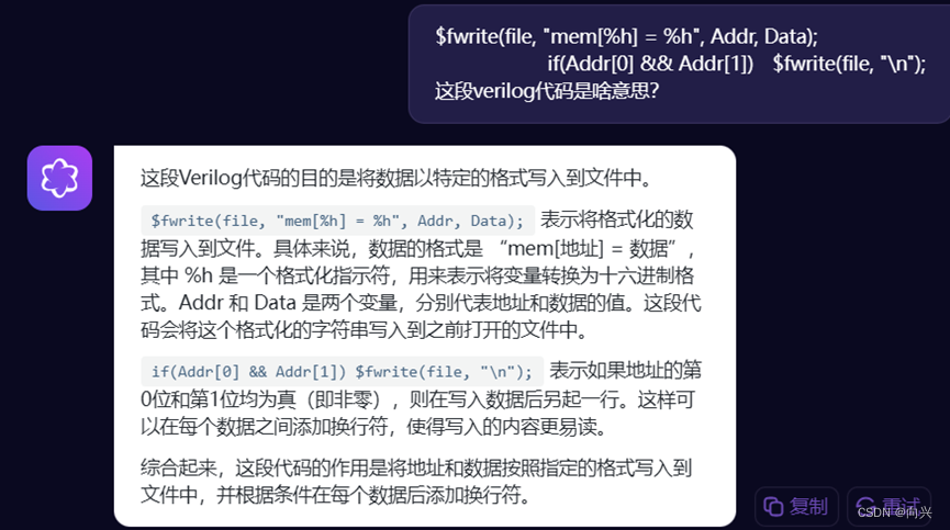
下面是chatgpt对这条语句的解释:

6.2,RTL代码
`timescale 1ns / 1ps
//
// Company:
// Engineer:
//
// Create Date: 2023/12/01 17:38:38
// Design Name:
// Module Name: sram
// Project Name:
// Target Devices:
// Tool Versions:
// Description:
//
// Dependencies:
//
// Revision:
// Revision 0.01 - File Created
// Additional Comments:
//
///* sram is Verilog HDL model for HM - 65162, 2K*8 bit Asynchronous(异步) CMOS
Static RAM. It is used in simulation to substitute the real RAM to verify whether
the writing or reading of the RAM is OK.
This module is a behavioral model for simulation only, not synthesizable. It's
writing and reading function are verified.
*/module sram(
Address, Data, SRG, SRE, SRW
);
input [10:0] Address;
input SRG; // output enable
input SRE; // chip enable
input SRW; // write enableinout [7:0] Data; // Buswire [10:0] Addr = Address;
reg [7:0] RdData;
reg [7:0] SramMem [0:'h7ff];
reg RdSramDly, RdFlip;
wire [7:0] FlpData;
wire [7:0] Data;reg WR_flag; // to judge the signals according to the specification of // HM-65162
integer i;wire RdSram = ~SRG & ~SRE;
wire WrSram = ~SRW & ~SRE;reg [10:0] DelayAddr;
reg [7:0] DelayData;
reg WrSramDly;integer file;assign FlpData = (RdFlip) ? ~RdData : RdData;
assign Data = (RdSramDly) ? FlpData : 'hz;/*
parameters of read circle
*/// 参数序号、最大或最小、参数含义
parameter TAVQV = 90, // 2, max, address access timeTELQV = 90, // 3, max, chip enable access timeTELQX = 5, // 4, min, chip enable output enable time TGLQV = 65, // 5, max, output enable access tiemTGLQX = 5, // 6, min, output enable output enable time TEHQZ = 50, // 7, max, chip enable output disable timeTGHQZ = 40, // 8, max, output enable output disable timeTAVQX = 5; // 9, min, output hold from address changeparameter TAVWL = 10, // 12, min, address setup timeTWLWH = 55, // 13, min, chip enable pulse setup time,// write enable pluse width,TWHAX = 15, // 14, min10, write enable read setup time,// 读上升沿后地址保留时间TWLQZ = 50, // 16, max, write enable output disable timeTDVWH = 30, // 17, min, data setup timeTWHDX = 20, // 18, min15, data hold timeTWHQX = 20, // 19, min0, write enable output enable time, 0TWLEH = 55, // 20, min, write enable pulse setup timeTDVEH = 30, // 21, min, chip enable data setup timeTAVWH = 70; // 22, min65, address valid to end of writeinitial beginfile = $fopen("ramlow.txt");if(!file) begin$display("Could not open the file.");$stop;end
endinitial beginfor(i = 0; i < 'h7ff; i = i + 1)SramMem[i] = i;// monitor($time, "DelayAddr = %h, DelayData = %h", DelayAddr, DelayData);
endinitial RdSramDly = 0;
initial WR_flag = 1;// READ CIRCLE
always@(posedge RdSram) #TGLQX RdSramDly = RdSram;
always@(posedge SRW) #TWHQX RdSramDly = RdSram;
always@(Addr) begin#TAVQX;RdFlip = 1;#(TGLQV - TAVQX); // address access timeif(RdSram)RdFlip = 0;
end always@(posedge RdSram) beginRdFlip = 1;#TAVQV; // output enable access timeif(RdSram) RdFlip = 0;
endalways@(Addr) #TAVQX RdFlip = 1;
always@(posedge SRG) #TEHQZ RdSramDly = RdSram;
always@(posedge SRE) #TGHQZ RdSramDly = RdSram;
always@(negedge SRW) #TWLQZ RdSramDly = 0;always@(negedge WrSramDly or posedge RdSramDly) RdData = SramMem[Addr];// WRITE CIRCLE
always@(Addr) #TAVWL DelayAddr = Addr; // Address setup
always@(Data) #TDVWH DelayData = Data; // Data setup
always@(WrSram) #5 WrSramDly = WrSram;
always@(Addr or Data or WrSram) WR_flag = 1;always@(negedge SRW) begin#TWLWH; // Write enable pulse widthif(SRW) beginWR_flag = 0;$display("ERROR! Can't write! Write enable time(W) is too short!");end
endalways@(negedge SRW) begin#TWLEH; // Write enable pulse setup timeif(SRE) beginWR_flag = 0;$display("ERROR! Can't write! write enable pulse setup time(E) is too short!");end
endalways@(posedge SRW) begin#TWHAX; // Write enable read setup timeif(DelayAddr !== Addr) beginWR_flag = 0;$display("ERROR! Can't write! Write enable read setup time is too short!");end
endalways@(Data)if(WrSram) begin#TDVEH; // chip enable data setup timeif(SRE) beginWR_flag = 0;$display("ERROR! Can't write! chip enable data setup time is too short!");end
endalways@(Data)if(WrSram) begin#TDVEH;if(SRW) beginWR_flag = 0;$display("ERROR! Can't write! chip enable data setup time is too short!");end
endalways@(posedge SRW) begin#TWHDX; // Data hold timeif(DelayData !== Data)$display("Warning! Data hold time is too short!");
endalways@(DelayAddr or DelayData or WrSramDly)if(WrSram && WR_flag) beginif(!Addr[5]) begin#15 SramMem[Addr] = Data;// $display("mem[%h] = %h", Addr, Data);$fwrite(file, "mem[%h] = %h", Addr, Data);if(Addr[0] && Addr[1]) $fwrite(file, "\n");endelse begin$fclose(file);$display("Please check the txt.");$stop;end
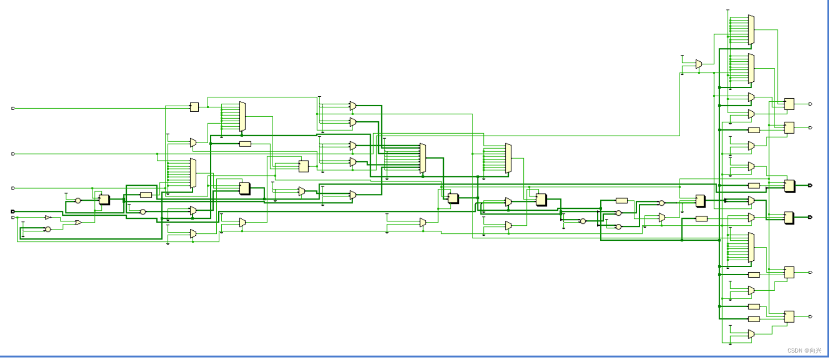
endendmodule7,vivado生成的RTL原理图
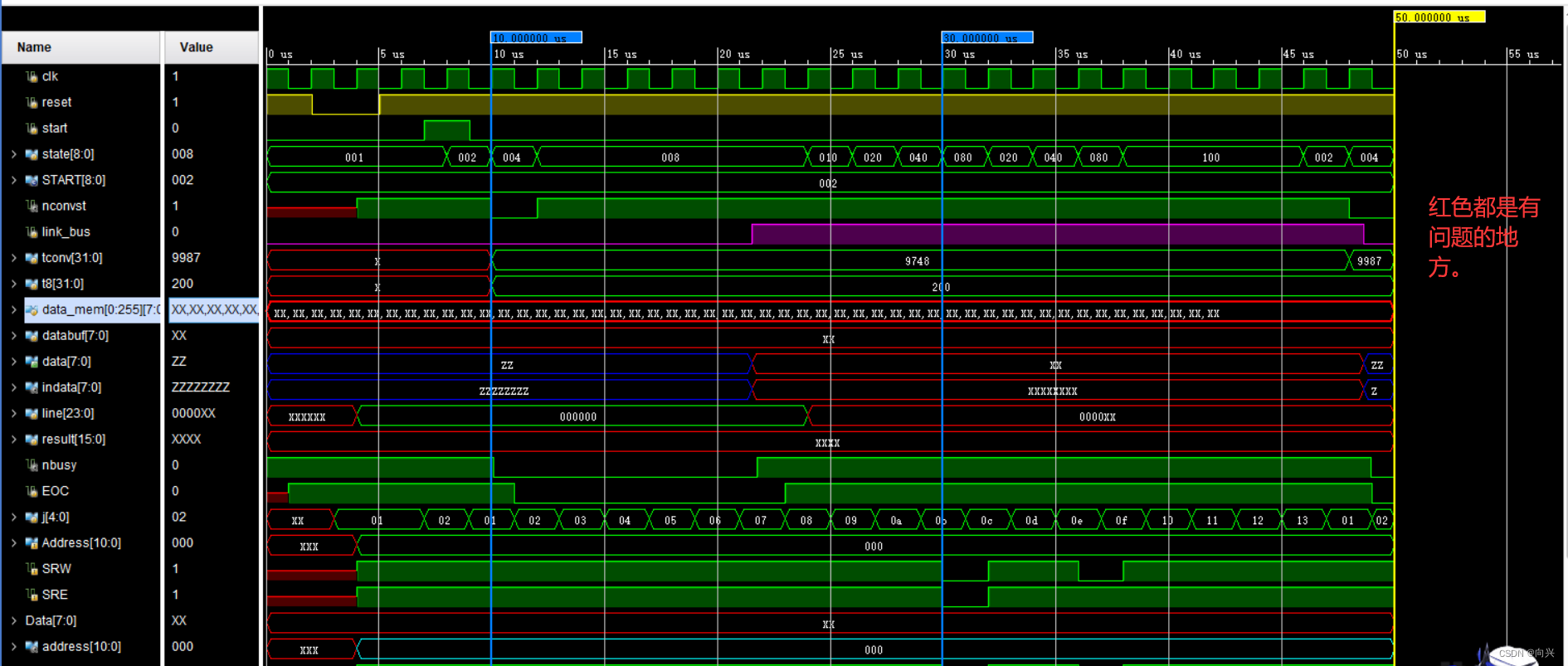
8,波形图